Creating a DUT
Open DUTs in the sidebar and click New DUT (also available from the home page). Each DUT represents a single board design — if you have multiple boards, create a separate DUT for each.
There are two ways to create a DUT, selectable from the tabs at the top.
From design files
The standard path: name your device, specify a revision, and upload your design files.
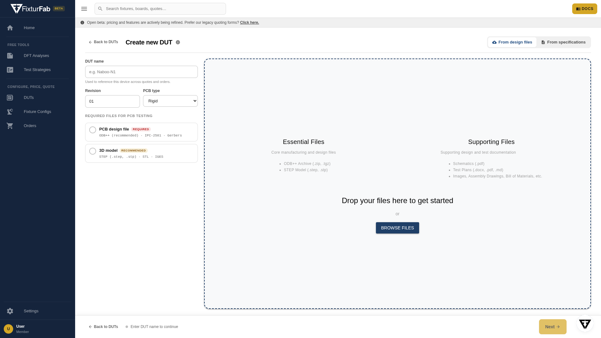
Two files matter most:
- PCB design package — ODB++ (recommended), IPC-2581, or Gerbers. This is what Studio parses into the board model: layout, test points, components, dimensions.
- 3D model — STEP (.step, .stp), STL, or IGES. Used for component-height awareness and pressure planning.
You can upload more than these — drop in an entire directory and Studio identifies what's relevant (it detects ODB++ archives, Gerber sets, and STEP models automatically). The more complete your file package, the better the downstream analysis. You can always add files later from the DUT's Files tab.
If you upload multiple PCB-type files, Studio asks which one is the authoritative PCB design before processing.
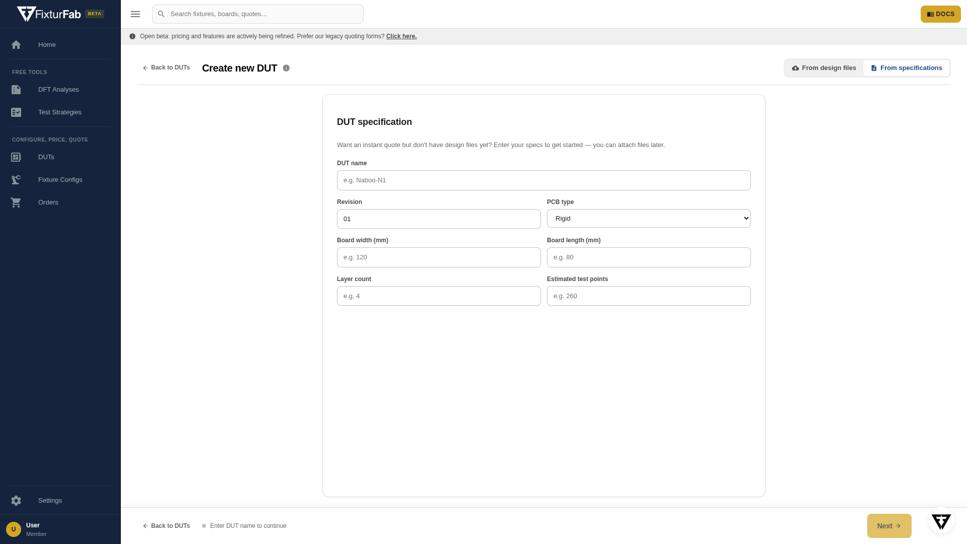
From specifications
No design files yet? Create the DUT from specifications instead — enter the board details manually and attach files later. This is useful early in a design cycle when you want pricing signals before the layout is final.
Processing
After creation, Studio processes the files in the background — parsing the PCB design, extracting board specifications, and rendering the layout. Each file shows its processing status on the DUT detail page, and the activity feed records what happened. Once files are processed you'll see the parsed board: dimensions, layer count, component count, and the interactive PCB layout.
From here, the next step is a test config — the DUT detail page prompts you once your files are ready.