

Appearance
Design for Test Report Summary
The DFT Report Summary page displays a preview of the configured Device Under Test (DUT) and a summary page of all the DUT characteristics, fixture information, and detected issues.
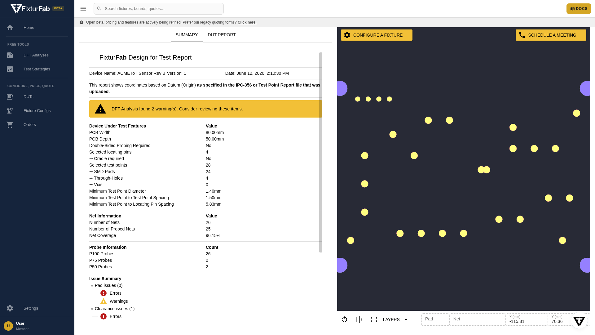
Report Summary
The top section of the DFT report summarizes the basic report information, such as the name of the DUT, date the report was created, and a status bar showing whether there are errors or warnings.

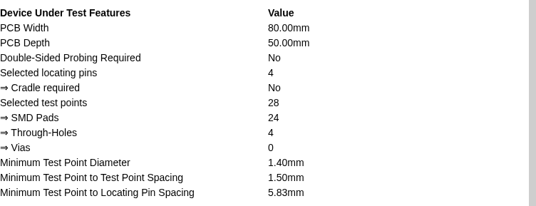
Device Under Test Features
The DUT Features section contains information that was identified from the IPC-356 Netlist file. This includes the following:
- DUT/PCB Dimensions
- Double-Sided Probing Requirements
- Locating Method
- Number and Type of Test Points
- Minimum Test Point Features
Net Information
The number of nets, number of probed nets, and net coverage is displayed in this section. While greater net coverage is better, functional test fixtures have the ability to test many of the non-accessed nets as long as a thoughtful test plan has been developed.

Probe Information
The type of probe that can be used is displayed in this section. In general, there are 3 different probe "types" that we use, these are referred to as P100, P75, and P50 probes.
The numeric value corresponds to the number of "mils" or 0.001in that is the minimum center to center test point spacing for the probe. So P100 probes can be placed 100mil (2.54mm) apart, P75 probes can be placed 75mil (1.9mm) apart, etc.
These counts are suggestions, and during the design of the fixture may change. For example, you may decide to use all P75 probes instead of P100 and P75 so that you only need to replace a single type of probe in the future.

Issue Summary
The Issue Tree will be displayed fully expanded. This will highlight all of the errors and warnings identified by the DFT tool.
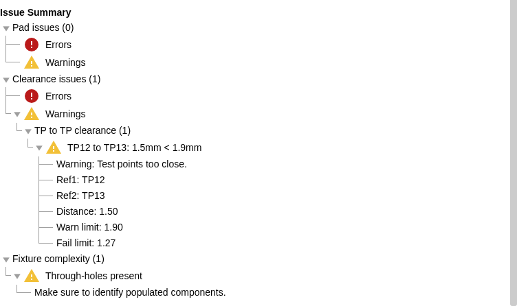
Issues will either be errors or warnings, to find out more about these issues, see this page.
Design Recommendations
Optimal test point specifications for reliable probing:
| Parameter | Ideal | Minimum |
|---|---|---|
| Spacing | 2.54mm (100mil) | 1.9mm (75mil) |
| Diameter | 1mm | 0.8mm |
| Clearance from components | N/A | 1.27mm (50mil) |
Additional recommendations:
- Same-side probing preferred — avoid double-sided probing approaches when possible.
- Mounting holes — include at least two holes at 1mm+ diameter for DUT locating.
- Test point placement — keep test points accessible and away from tall components.
Common Questions
What does "test coverage" mean?
Test coverage represents the percentage of your design's nets that can be accessed through probe contact. Higher coverage means more comprehensive electrical testing is possible. 100% coverage isn't always necessary — focus coverage on critical signals and power rails.
My coverage is lower than expected. What can I do?
Common causes of low coverage:
- Test points too close together (increase spacing to 2.54mm minimum)
- Test points obscured by tall components (relocate test points)
- Missing test points on critical nets (add dedicated test pads)
- Double-sided designs requiring probing from both sides (consider single-sided access)
How do I improve my DFT score?
For future board revisions:
- Add dedicated test pads on critical nets
- Maintain minimum 2.54mm spacing between test points
- Keep test points 1.27mm away from component bodies
- Include mounting holes for DUT locating
- Consider test requirements during component placement