Test Point Carrier Boards
A Test Point Carrier Board, also commonly referred to as an interface or wireless board, is a custom PCB that is designed to route test probes to any connector, circuitry, or instrumentation that is needed to implement a test.
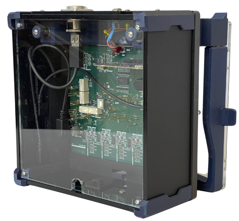
The image above shows the Test Point Carrier Board for testing FixturFab's FixturCtrl USB Hub. This TPCB contains several different subcircuits related to testing, including:
- Continuity Testing and Power Supply Mux
- USB Hub Communication and RP2040 Programming
- Downstream USB Device and Load Testing
Designing Your Own Test Point Carrier Board
FixturFab is more than willing to support you in designing your own TPCB. In this case, the typical design process is as follows:
- Download TPCB Design Assets for your specific fixture
- Download the Board Outline according to the fixture that you are designing
- Download the Receptacle Footprint Library
- These are provided in Kicad format and can be imported to any design tool that you use
- Create your schematic
- Create the initial layout of the TPCB
- Initial Layout Review
- Share STEP and initial Gerbers with FixturFab
- FixturFab reviews layout and provides any feedback on component placement, test point placement, etc.
- Complete routing
- Route all of the signals on the TPCB
- FixturFab recommends routing differential, high-power, and any sensitive signals by hand
- Auto-router can be used for anything else
- Share complete TPCB STEP and Gerbers with FixturFab
- FixturFab reviews layout and confirms that the board will fit mechanically
- Order the TPCB
- Place order for the PCB fabrication and assembly
- Ship assembled TPCB to FixturFab
- FixturFab 3410 Woodland Park Ave N Suite C Seattle, WA 98103
- FixturFab integrates the TPCB into your fixture and completes assembly and QA
- Fixture is shipped to you
Production vs Development Test Point Carrier Boards (TPCBs)
While the same TPCB designs can be used, the receptacle footprints change on the production test fixtures. The Development TPCBs utilize through-holes, which the test probe receptacles solder to, while the Production TPCBs use SMD pads, which are compatible with wireless receptacles.
Sub-Probe Plate
On Production Test Fixtures that use wireless receptacles, a sub-probe plate is used to mount the receptacles to the fixture. This plate is mounted to probe plate using standoffs, and the TPCB is mounted to the sub-probe plate.
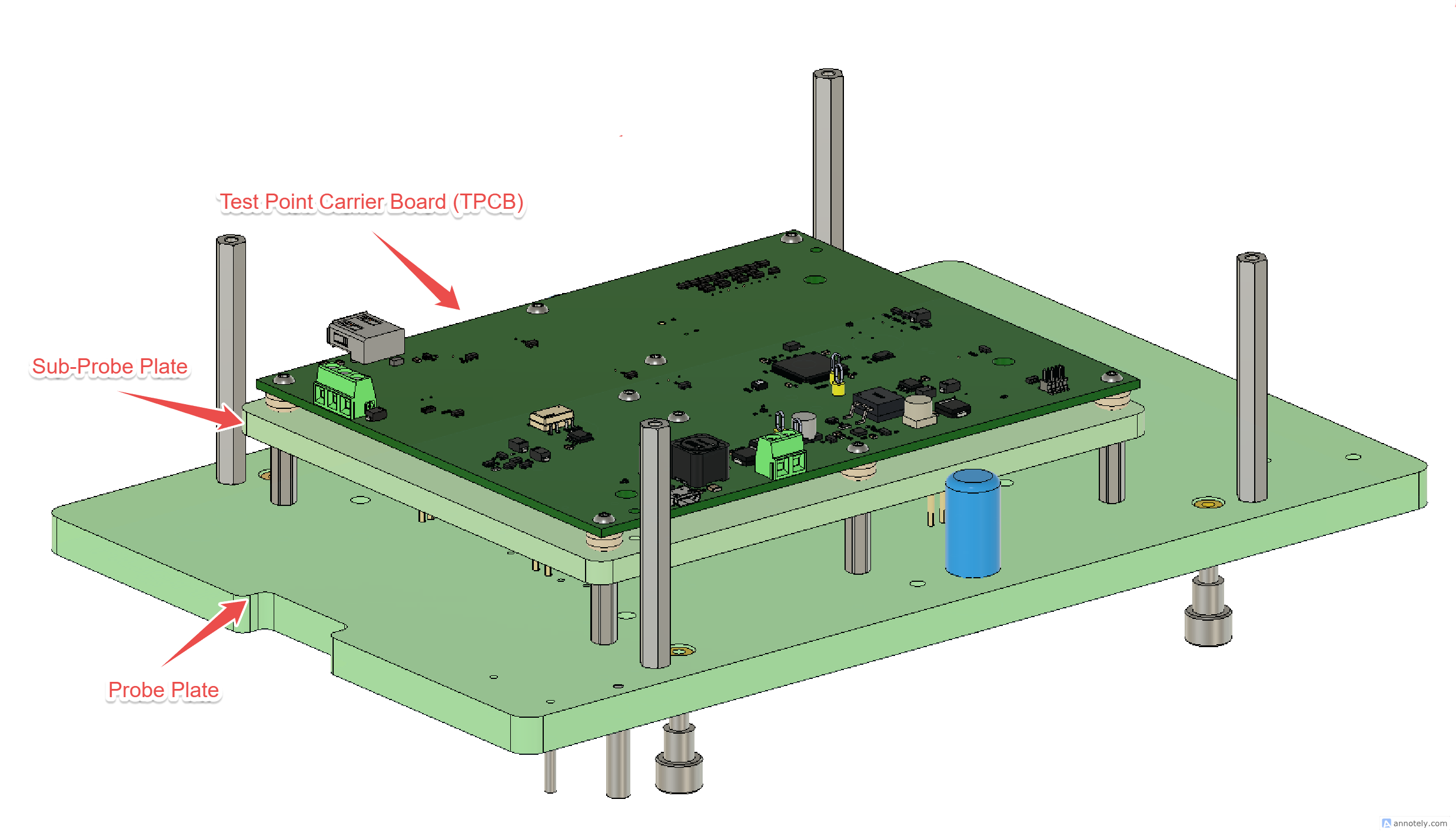
The mounting holes on the sub-probe plate should be 6mm in diameter, which allows for a 3D-printed spacer to be press fit into the hole, providing the correct offset for the working stroke of the spring-loaded pin on the wireless receptacle.
Design Guidelines and Best Practices
This section provides comprehensive guidance for designing TPCBs that meet both electrical and mechanical requirements.
Test Point Location and Layer
Depending on whether you are probing the Top or Bottom side of the DUT, you may need to mirror the test points on your TPCB.
We find it easiest to place the Test Points on the Bottom side of the TPCB, and all components on the Top. If following this approach, you will need to mirror the test points if the Top side of the DUT is being probed.
TPCB Alignment
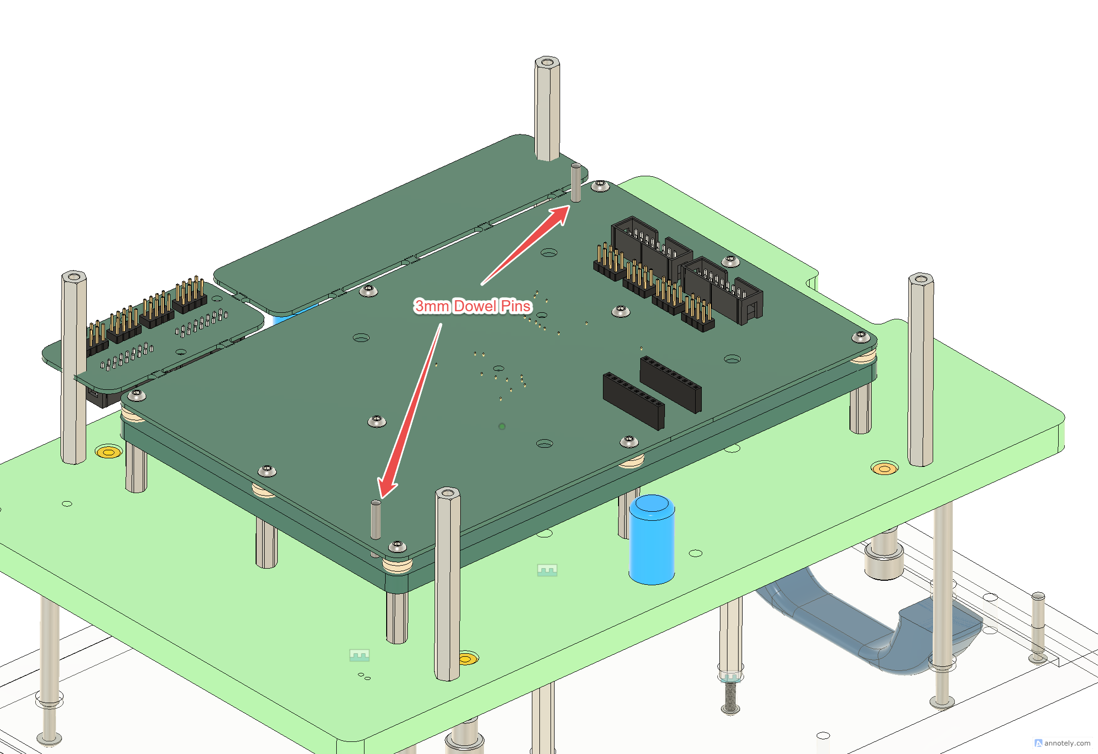
To align the TPCB, place 2 - 3mm NPTH holes in opposite corners. Place them as shown below to prevent the TPCB from being attached in the wrong orientation.
TPCB Board Outlines
The outline of each TPCB varies depending on the fixture that it will be mounted within. Here are DXF and PDF files for our commonly used fixture bases.
Development Fixtures and Cartridges
- Dev
- Dev XL
- Dev Pro
- Dev Pro XL
Ingun Fixtures and Cartridges
- MA260
- MA11
- MA12
- MA13
- MA14
Receptacle and Guide Pin Footprints
Open Source KiCad Library
We have a KiCad Library for Schematic Symbols and Footprints available here.
Recommended Receptacle Footprints
There are four common footprints that we use for almost all receptacles. These are shown below.
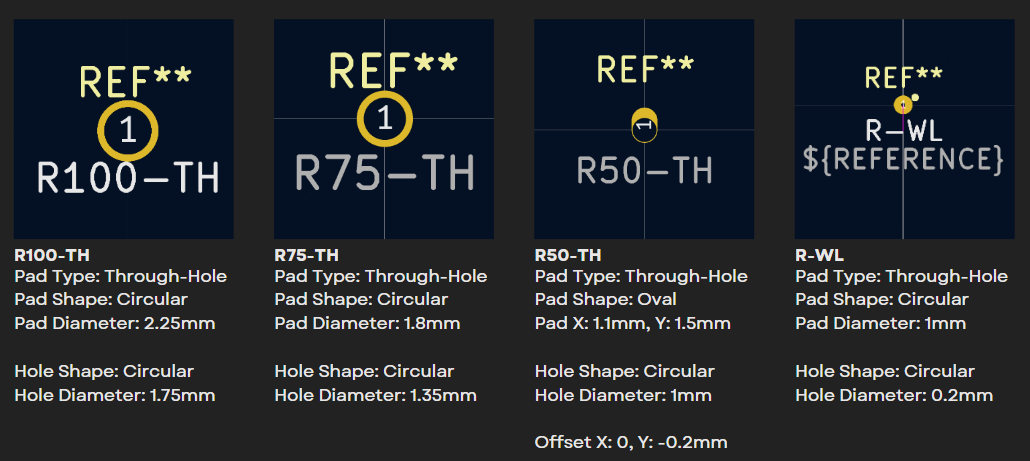
The R50-TH, R75-TH, and R100-TH footprints are through-hole and designed so that the receptacle will be inserted through the hole and then soldered to the board. This style of receptacle is commonly used in our development style fixtures.
The R-WL footprint is for use with wireless receptacles, which feature a secondary pogo-pin at the bottom of the receptacle. This footprint is still a through-hole, with a small 0.2mm hole through the board. This enables you to still probe the test point from the bottom of the TPCB while you are bringing up or debugging the fixture.
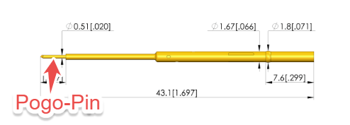
These receptacles are used on all of our Production Test Fixtures. This allows for the TPCB to be easily replaced and maintained due to no solder being used to connect the receptacles to the TPCB.
Guide Pin Footprints
Spring Guide Pins are one of our favorite methods to use for locating a DUT within a fixture. They support a wide variety of hole dimensions that can be used with mounting or tooling holes on the DUT.

A side effect of using a Spring Guide Pin is that the pin extends down as the tip is compressed. This requires a hole to be placed on the TPCB to ensure there isn't any interference.
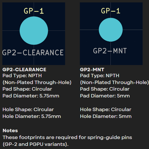
If dowel pins or tooling pins will be used to locate the DUT, a footprint doesn't need to be placed on the TPCB.
App: Ingun Inductive Fixture Switch
One of our favorite accessories to integrate into an Ingun Fixture Base is an Inductive Switch. This integrates into the fixture base and enables you to easily determine if the fixture is closed.
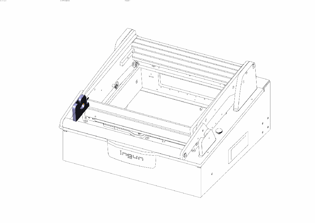
The sensor included in this accessory is a IFM IY5052 Inductive Sensor. This can be powered with 10-30VDC, and has a PNP Output.
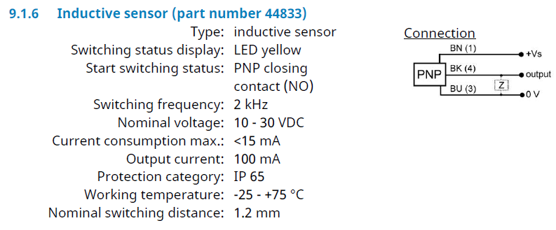
To interface with this sensor, we commonly use a 3-pin terminal block with the following pinout:
| Pin | TPCB Connection | Switch Wire Color |
|---|---|---|
| 1 | 12V | Brown (BN) |
| 2 | SW | Black (BK) |
| 3 | GND | Blue (BU) |
We use a voltage divider to adjust the 12V output (showing that the fixture is closed) to whatever logic level is being used by the instrumentation in the fixture.
Common connectors we've used are:
